

- About us
- Our Profile
- Qualification certificate
- Board of Governing
- Executive Management Team
- Affiliation/ Partners
- Milestones
- Global Network
- Corporate Social Responsibility
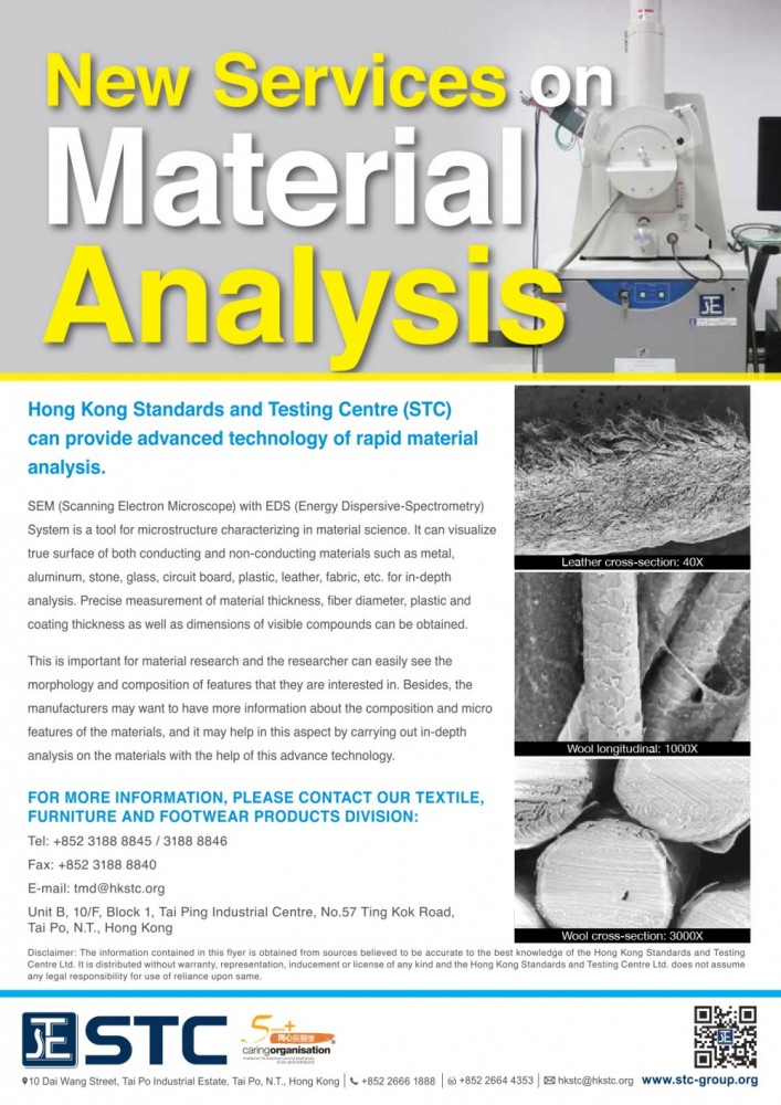
- Services
- Testing
- Inspection
- Certification
- Other Services
- Media Centre
- Corporate News & Events
- Latest promotion
- Market & industry info
- Download Area
- Application Form
- Reference Guide
- Contact Us
- Report Status
- Career Opportunities
- Terms of Use
- Privacy Statement